Technology & Products
[SDI Focus] Slurries Gain Traction as Semiconductor advances
2025.04.08
With the advent of the AI era, high performance semiconductors capable of rapidly reading and writing large volumes of data are becoming increasingly important. These high performance chips enhance integration by stacking circuit layers on the wafer. For a stable layering, a planarization process is required for each layer—and the key material in this process is a slurry.
Slurries are used in the CMP (Chemical-Mechanical Polishing/Planarity) process* to polish layers. They consist of an aqueous solution with chemical additives and dispersed abrasive particles. In the CMP process, chemical additives in the slurry first soften the hard layer through chemical reactions. Then, nano-scale particles physically smooth the layer surface.
*CMP Process: a chemical and mechanical method of polishing (or planarization) the surface of a semiconductor wafer.
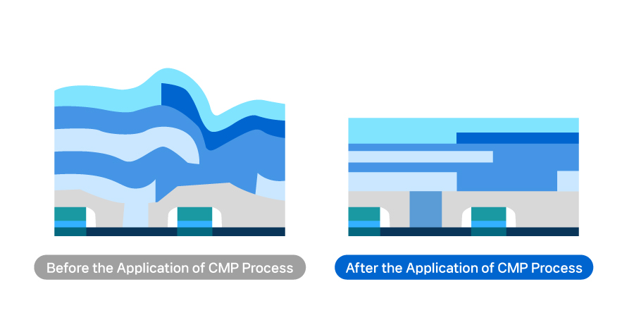
[The planarization (CMP) process uses a slurry to polish a wafer’s surface]
Slurries are divided into metal slurries and non-metal slurries depending on the layer’s material. Metal slurries are used to polish metal layers, while non-metal slurries are used to polish non-metal slurries. The metal layer is a material used primarily for semiconductor wiring, such as tungsten (W) and copper (Cu). The non-metal layer includes silicon oxide, which can insulate between these metal wires, and organic films, a newer material that has been introduced recently.
SAMSUNG SDI started developing slurries in 1998 and has been expanding its business since 2002, starting with oxide slurries. In particular, tungsten slurries, which have been sold since 2003, have recently been developed and mass-produced to greatly increase the convenience and efficiency of the CMP process.
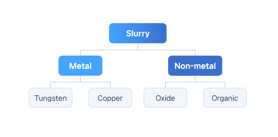
[Types of slurries]
The CMP process is typically divided into the bulk* and BM* (Barrier Metal) areas depending on the stage of the process. The bulk process polishes only the target layer, and the BM process polishes both the target and bottom layers simultaneously. Traditionally, a separate slurry is used to polish each layer area. However, SAMSUNG SDI’s tungsten slurries can be used for all stages of the process, increasing efficiency and productivity by reducing defect rates.
*Bulk/BM areas: Before the CMP process, metal layers are categorized into the polish-targeted metal bulk area and the BM (Barrier Metal) area that separates the metal and non-polish areas.
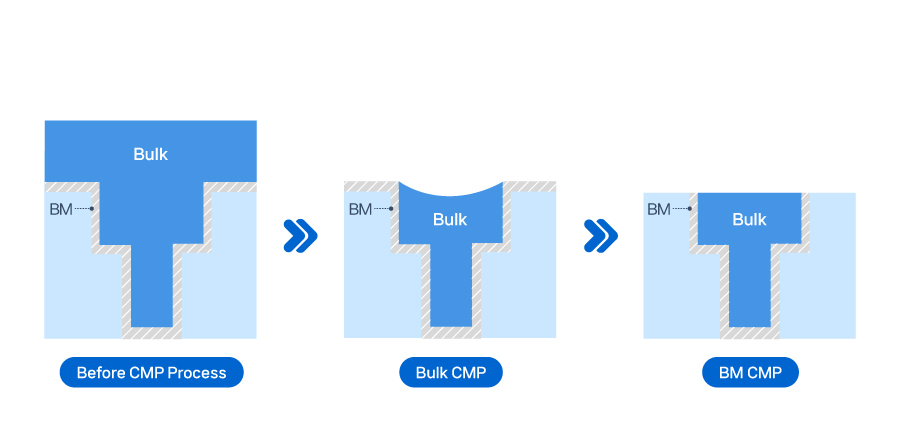
[The planarization process in the bulk and BM areas]
[SAMSUNG SDI’s tungsten slurry]
SAMSUNG SDI is currently working on the R&D of next-generation tungsten slurries that can prevent defects based on their high purity characteristics and unique chemical additives. Furthermore, SAMSUNG SDI plans to expand the R&D of various slurries tailored to customer demands, such as copper slurry, oxide slurry, and organic slurry.

SAMSUNG SDI Newsroom
We deliver the latest news and issues coming out of SAMSUNG SDI.